HDLbits exercises 10(LATCHES AND FLIP-FLOPS后半部分题)
目录
1\ DFF+GATE
2\ MUX AND DFF1
3\ MUX AND DFF2
4\ DFFS AND GATE
5\ CREATE CIRCUIT FROM TRUTH TABLE
6\ DETECT AN EDGE
7\ DETECT BOTH EDGES
8\ EDGE CAPTURE REGISTER
9\ DUAL-EDGE TRIGGERED FLIP-FLOP
1\ DFF+GATE
Implement the following circuit:

HINT:
直接写即可,不用中间量。
CORRECT:
module top_module (
input clk,
input in,
output out);
always@(posedge clk)
begin
out<=in^out;
end
endmodule
2\ MUX AND DFF1
Taken from ECE253 2015 midterm question 5
Consider the sequential circuit below:
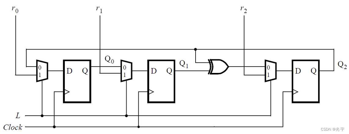
Assume that you want to implement hierarchical Verilog code for this circuit, using three instantiations of a submodule that has a flip-flop and multiplexer in it. Write a Verilog module (containing one flip-flop and multiplexer) named top_module for this submodule.
HINT:
摸摸,别害怕,这里只是让你设计一个子模块,没让你搭整个电路~
CORRECT:
module top_module (
input clk,
input L,
input r_in,
input q_in,
output reg Q);
always @(posedge clk)
begin
Q<=L?r_in:q_in;
end
endmodule
3\ MUX AND DFF2
Consider the n-bit shift register circuit shown below:
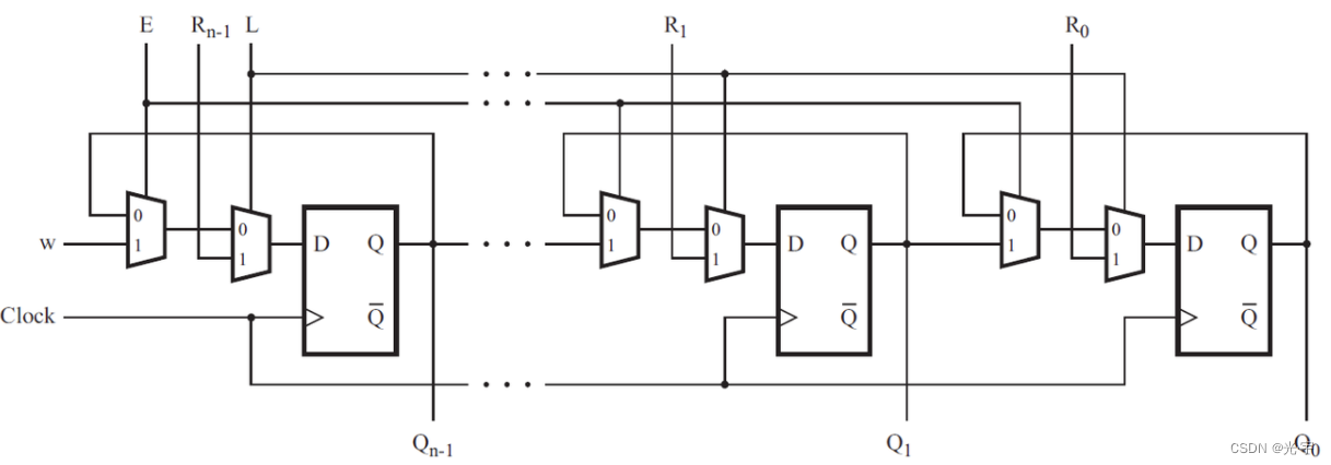
Write a Verilog module named top_module for one stage of this circuit, including both the flip-flop and multiplexers.
CORRECT:
module top_module (
input clk,
input w, R, E, L,
output Q
);
always@(posedge clk)
begin
Q<=L?R:(E?w:Q);
end
endmodule
4\ DFFS AND GATE
Given the finite state machine circuit as shown, assume that the D flip-flops are initially reset to zero before the machine begins.
Build this circuit.

HINT:
Be careful with the reset state. Ensure that each D flip-flop's Q output is really the inverse of its Q output, even before the first clock edge of the simulation.
ERRO:
module top_module (
input clk,
input x,
output z
);
reg q1,q2,q3;
always@(posedge clk)
begin
q1<=x^q1;
q2<=x&!q2;
q3<=x|!q3;
z<=!(q1|q2|q3); ///应当放always外头,z不需要触发条件。
end
endmodule
ERRO
module top_module (
input clk,
input x,
output z
);
reg q1,q2,q3;
always@(posedge clk)
begin
q1<=x^q1;
q2<=x&!q2;
q3<=x|!q3;
end
assign z<=!(q1|q2|q3);///此处要用阻塞赋值
endmodule
CORRECT1:
module top_module (
input clk,
input x,
output z
);
reg q1,q2,q3;
always@(posedge clk)
begin
q1<=x^q1;
q2<=x&!q2;
q3<=x|!q3;
end
assign z=!(q1|q2|q3);
endmodule
CORRECT2:这种写法可能暂时复杂,但是后期调试简单。

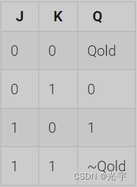
5\ CREATE CIRCUIT FROM TRUTH TABLE
A JK flip-flop has the below truth table. Implement a JK flip-flop with only a D-type flip-flop and gates. Note: Qold is the output of the D flip-flop before the positive clock edge.
CORRECT:
module top_module (
input clk,
input j,
input k,
output Q);
always@(posedge clk)begin
Q<=j?(k?!Q:1):(k?0:Q);
end
endmodule
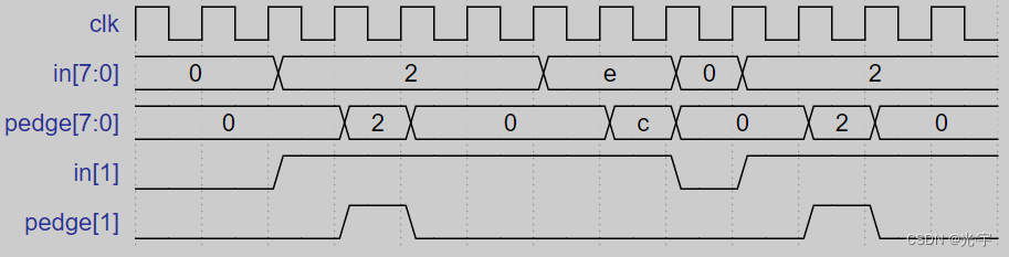
6\ DETECT AN EDGE
For each bit in an 8-bit vector, detect when the input signal changes from 0 in one clock cycle to 1 the next (similar to positive edge detection). The output bit should be set the cycle after a 0 to 1 transition occurs.(对于8位向量中的每一位,检测输入信号在一个时钟周期内从0变为下一个时钟周期内的1(类似于正边缘检测)。输出位应该在0到1转换发生后的周期设置。)
Here are some examples. For clarity, in[1] and pedge[1] are shown separately.
HINT:
这个题要求进行边沿检测,这需要一些预备知识,详见链接:
FPGA基础学习——Verilog实现的边沿检测(上升沿下降沿检测)及Modelsim仿真_Fighting_XH的博客-CSDN博客_verilog边沿检测
CORRECT:
module top_module (
input clk,
input [7:0] in,
output [7:0] pedge
);
reg [7:0] temp_in;
always @(posedge clk) begin
temp_in <= in; 把上一个时钟的in存到中间变量里
pedge <= ~temp_in & in; //把当前的in和上一个时钟的in的反进行与运算,以此检测是否有上升沿
end
endmodule
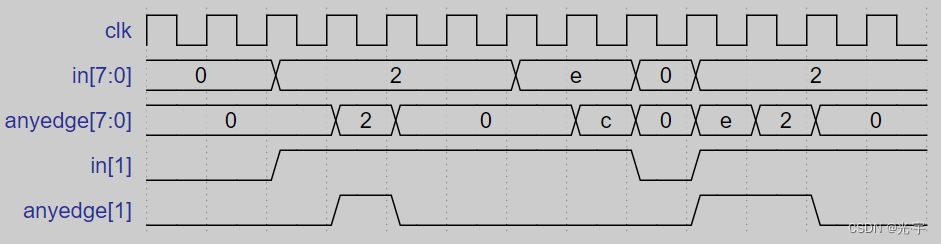
7\ DETECT BOTH EDGES
For each bit in an 8-bit vector, detect when the input signal changes from one clock cycle to the next (detect any edge). The output bit should be set the cycle after a 0 to 1 transition occurs.
Here are some examples. For clarity, in[1] and anyedge[1] are shown separately
CORRECT:
module top_module (
input clk,
input [7:0] in,
output [7:0] anyedge
);
reg [7:0] a;
always @(posedge clk)begin
a<=in;
anyedge<=a&~in|~a∈
end
endmodule
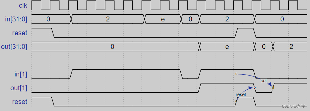
8\ EDGE CAPTURE REGISTER
For each bit in a 32-bit vector, capture when the input signal changes from 1 in one clock cycle to 0 the next. "Capture" means that the output will remain 1 until the register is reset (synchronous reset).(对于32位向量中的每个位,当输入信号在一个时钟周期内从1变为下一个时钟周期内的0时捕获。“Capture”意味着输出将保持1,直到寄存器重置(同步重置)。)
Each output bit behaves like a SR flip-flop: The output bit should be set (to 1) the cycle after a 1 to 0 transition occurs. The output bit should be reset (to 0) at the positive clock edge when reset is high. If both of the above events occur at the same time, reset has precedence. In the last 4 cycles of the example waveform below, the 'reset' event occurs one cycle earlier than the 'set' event, so there is no conflict here.(每个输出位的行为就像一个SR触发器:输出位应该在1到0转换发生后的周期设置(1)。当复位值高时,输出位应该在正时钟边缘复位(到0)。如果上述两个事件同时发生,则reset优先。在下面示例波形的最后4个周期中,'reset'事件比'set'事件早发生一个周期,所以这里没有冲突。)
In the example waveform below, reset, in[1] and out[1] are shown again separately for clarity.
ERRO:
module top_module (
input clk,
input reset,
input [31:0] in,
output [31:0] out
);
reg [31:0] a;
always@(posedge clk)
begin
if(reset)
begin
out<=32'b0;
end
else
begin
a<=in;
out<=~in&a;
end
end
endmodule
CORRECT:
module top_module (
input clk,
input reset,
input [31:0] in,
output [31:0] out
);
reg [31:0] a;
always@(posedge clk)
begin
a<=in; ///无论到什么时候,应该先记录前一时刻的状态,不用管reset状态。
if(reset)
begin
out<=32'b0;
end
else
begin
out<=~in&a|out;///后面的或运算是因为要进行“捕获”,只要~in&a等于1,那么1无论和谁做或运算,都是1,这就相当于是捕获了。
end
end
endmodule
9\ DUAL-EDGE TRIGGERED FLIP-FLOP
You're familiar with flip-flops that are triggered on the positive edge of the clock, or negative edge of the clock. A dual-edge triggered flip-flop is triggered on both edges of the clock. However, FPGAs don't have dual-edge triggered flip-flops, and always @(posedge clk or negedge clk) is not accepted as a legal sensitivity list.
Build a circuit that functionally behaves like a dual-edge triggered flip-flop:
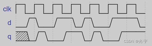
(Note: It's not necessarily perfectly equivalent: The output of flip-flops have no glitches(故障), but a larger combinational circuit that emulates(仿真) this behaviour might. But we'll ignore this detail here.)
HINT:
- You can't create a dual-edge triggered flip-flop on an FPGA. But you can create both positive-edge triggered and negative-edge triggered flip-flops.
- This problem is a moderately difficult circuit design problem, but requires only basic Verilog language features. (This is a circuit design problem, not a coding problem.) It may help to first sketch a circuit by hand before attempting to code it.
(不能在FPGA上创建双边沿触发触发器。但您可以创建正边触发和负边触发的触发器。这个问题是一个中等难度的电路设计问题,但只需要基本的Verilog语言特性。(这是一个电路设计问题,不是编码问题。)在对电路进行编码之前,先用手绘草图可能会有所帮助。)
虽然一个always里不能有clk,但是我可以有俩always啊。。。
CORRECT:
module top_module (
input clk,
input d,
output q
);
reg q1,q2;
always @(posedge clk) begin
q1<=d;
end
always @(negedge clk) begin
q2<=d;
end
assign q = clk?q1:q2;
endmodule